From the previous blog, we already know about FPGA, like how it works, its structure, and its type. It means we already know the basic things about FPGA but let’s know some more facts about FPGA.
FPGA Program
FPGA programming uses an HDL to alter circuits based on the capabilities desired for the device. Because you are not building a programme that will execute sequentially, the technique differs from programming a GPU or CPU.
Rather, you’re using an HDL to design circuits and physically alter the hardware to accomplish your goals.
Writing code that is converted into a binary file and placed into the FPGA is similar to programming software.
However, instead of merely optimising the device to execute software, the HDL makes actual modifications to the hardware.
Using Xilinx as an example, we will learn how binaries are uploaded and how to construct a binary.
Verilog code for PWM generator
The PWM (Pulse Width Modulation) generator in Verilog generates a 10MHz PWM signal with a configurable duty cycle. The duty cycle of the PWM signal is controlled by two debouncing buttons. The first push button increases the duty cycle by 10%, while the second button decreases the duty cycle by 10%.
//Verilog code for PWM Generator with variable Duty Cycle
// Two debounced buttons are used to control the duty cycle (step size: 10%)
module PWM_Generator_Verilog
 (
 clk, // 100MHz clock input
 increase_duty, // input to increase 10% duty cycle
 decrease_duty, // input to decrease 10% duty cycle
 PWM_OUT // 10MHz PWM output signal
    );
 input clk;
 input increase_duty;
 input decrease_duty;
 output PWM_OUT;
 wire slow_clk_enable; // slow clock enable signal for debouncing FFs
 reg[27:0] counter_debounce=0;// counter for creating slow clock enable signals
 wire tmp1,tmp2,duty_inc;// temporary flip-flop signals for debouncing the increasing button
 wire tmp3,tmp4,duty_dec;// temporary flip-flop signals for debouncing the decreasing button
 reg[3:0] counter_PWM=0;// counter for creating 10Mhz PWM signal
 reg[3:0] DUTY_CYCLE=5; // initial duty cycle is 50%
  // Debouncing 2 buttons for inc/dec duty cycle
  // Firstly generate slow clock enable for debouncing flip-flop (4Hz)
 always @(posedge clk)
 begin
   counter_debounce <= counter_debounce + 1;
   //if(counter_debounce>=25000000) then
   // for running on FPGA -- comment when running simulation
   if(counter_debounce>=1)
   // for running simulation -- comment when running on FPGA
    counter_debounce <= 0;
 end
 // assign slow_clk_enable = counter_debounce == 25000000 ?1:0;
 // for running on FPGA -- comment when running simulation
 assign slow_clk_enable = counter_debounce == 1 ?1:0;
 // for running simulation -- comment when running on FPGA
 // debouncing FFs for increasing button
 DFF_PWM PWM_DFF1(clk,slow_clk_enable,increase_duty,tmp1);
 DFF_PWM PWM_DFF2(clk,slow_clk_enable,tmp1, tmp2);
 assign duty_inc =  tmp1 & (~ tmp2) & slow_clk_enable;
 // debouncing FFs for decreasing button
 DFF_PWM PWM_DFF3(clk,slow_clk_enable,decrease_duty, tmp3);
 DFF_PWM PWM_DFF4(clk,slow_clk_enable,tmp3, tmp4);
 assign duty_dec =  tmp3 & (~ tmp4) & slow_clk_enable;
 // vary the duty cycle using the debounced buttons above
 always @(posedge clk)
 begin
   if(duty_inc==1 && DUTY_CYCLE <= 9)
    DUTY_CYCLE <= DUTY_CYCLE + 1;// increase duty cycle by 10%
   else if(duty_dec==1 && DUTY_CYCLE>=1)
    DUTY_CYCLE <= DUTY_CYCLE - 1;//decrease duty cycle by 10%
 end
// Create 10MHz PWM signal with variable duty cycle controlled by 2 buttons
 always @(posedge clk)
 begin
   counter_PWM <= counter_PWM + 1;
   if(counter_PWM>=9)
    counter_PWM <= 0;
 end
 assign PWM_OUT = counter_PWM < DUTY_CYCLE ? 1:0;
endmodule
// Debouncing DFFs for push buttons on FPGA
module DFF_PWM(clk,en,D,Q);
input clk,en,D;
output reg Q;
always @(posedge clk)
begin
 if(en==1) // slow clock enable signal
  Q <= D;
end
endmodule
Testbench:
`timescale 1ns / 1ps
// fpga4student.com: FPGA Projects, Verilog projects, VHDL projects
// Verilog project: Verilog testbench code for PWM Generator with variable duty cycle
module tb_PWM_Generator_Verilog;
 // Inputs
 reg clk;
 reg increase_duty;
 reg decrease_duty;
 // Outputs
 wire PWM_OUT;
 // Instantiate the PWM Generator with variable duty cycle in Verilog
 PWM_Generator_Verilog PWM_Generator_Unit(
  .clk(clk),
  .increase_duty(increase_duty),
  .decrease_duty(decrease_duty),
  .PWM_OUT(PWM_OUT)
 );
 // Create 100Mhz clock
 initial begin
 clk = 0;
 forever #5 clk = ~clk;
 end
 initial begin
  increase_duty = 0;
  decrease_duty = 0;
  #100;
    increase_duty = 1;
  #100;// increase duty cycle by 10%
    increase_duty = 0;
  #100;
    increase_duty = 1;
  #100;// increase duty cycle by 10%
    increase_duty = 0;
  #100;
    increase_duty = 1;
  #100;// increase duty cycle by 10%
    increase_duty = 0;
  #100;
    decrease_duty = 1;
  #100;//decrease duty cycle by 10%
    decrease_duty = 0;
  #100;
    decrease_duty = 1;
  #100;//decrease duty cycle by 10%
    decrease_duty = 0;
  #100;
    decrease_duty = 1;
  #100;//decrease duty cycle by 10%
    decrease_duty = 0;
 end
endmodule
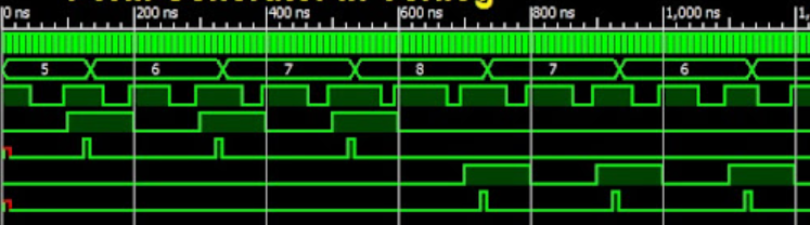
The Simulation waveform for the PWM generator in VHDL is shown in the below figure.
Blinking the LED with FPGA
So today we will discuss something more about the FPGA with some basic examples.
A hello world program for any hardware-based software is a LED – flashing example. So today we’ll be blinking the LED with FPGA. This example will suit Verilog’s examples.
This section demonstrates how to write Verilog code that blinks an LED at a set frequency. Whenever a design code is created, the FPGA designer must guarantee that it operates as planned.
This lesson is divided into two parts:
- HDL design
- HDL simulation
These both are essential for effective FPGA development. When FPGA designers are pressured for time, they may attempt to bypass step two, code simulation.
Design
So, before beginning the design process, it is critical to carefully select the product that will be used in blinking LEDs.
Create an HDL code to blink an LED at a specific frequency of 100, 50, 10, or 1 Hz. The LED will be set to a 50% duty cycle for each of the blink frequencies. That means it will be on half the time.
The LED frequency will be determined by two switches that are FPGA inputs. To turn on the LED, there is an extra switch called LED_EN that must be set to ‘1’. A 25 MHz oscillator will power the FPGA.
Let’s start with the frequency selector’s truth table:
| Enable | Switch 1 | Switch 2 | LED drive Frequency |
| 0 | – | – | (disabled) |
| 1 | 0 | 0 | 100 Hz |
| 1 | 0 | 1 | 50 Hz |
| 1 | 1 | 0 | 10 Hz |
| 1 | 1 | 1 | 1 Hz |
There will be four inputs and one output for this to operate properly. The signals will be as follows:
| Signal Name | Direction | Explanation |
| i_clock | Input | 25 MHz Clock |
| i_enable | Input | Enable switch |
| i_switch_1 | Input | Truth table Switch 1 |
| i_switch_2 | Input | Truth table Switch 2 |
| o_led_drive | Output | Signal driving LED |
There are four concurrent counter processes for the design. This implies that they are all active at the same time.
The switches solely serve to specify which output should be used. They build a device known as a multiplexer.
A multiplexer, often known as a mux, is a selector that chooses one of several inputs to propagate or pass to the output. It is a combinatorial piece of logic, which means it does not need a clock to function.
The design is seen in the diagram below. Spend some time considering how you may put this concept into action.
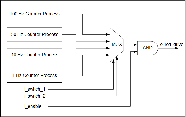
Fig 1: Block Diagram – LED Blink Program
Simulation
Below is the Verilog of the above-explained circuit.
module tutorial_led_blink
  (
   i_clock,
   i_enable,
   i_switch_1,
   i_switch_2,
   o_led_drive
   );

  input i_clock;
  input i_enable;
  input i_switch_1;
  input i_switch_2;
  output o_led_drive;

  			// Constants (parameters) to create the frequencies needed:
 			 // Input clock is 25 kHz, chosen arbitrarily.
 			 // Formula is: (25 kHz / 100 Hz * 50% duty cycle)
  			// So for 100 Hz: 25,000 / 100 * 0.5 = 125
  parameter c_CNT_100HZ = 125;
  parameter c_CNT_50HZ  = 250;
  parameter c_CNT_10HZ  = 1250;
  parameter c_CNT_1HZ   = 12500;

 			 // These signals will be the counters:
  reg [31:0] r_CNT_100HZ = 0;
  reg [31:0] r_CNT_50HZ = 0;
  reg [31:0] r_CNT_10HZ = 0;
  reg [31:0] r_CNT_1HZ = 0;

 			 // These signals will toggle at the frequencies needed:
  reg        r_TOGGLE_100HZ = 1'b0;
  reg        r_TOGGLE_50HZ  = 1'b0;
  reg        r_TOGGLE_10HZ  = 1'b0;
  reg        r_TOGGLE_1HZ   = 1'b0;

  			// One bit select
  reg        r_LED_SELECT;
  wire       w_LED_SELECT;


begin

  			// All always blocks toggle a specific signal at a different frequency.
 			 // They all run continuously even if the switches are
 			 // not selecting their particular output.

  always @ (posedge i_clock)
    begin
      if (r_CNT_100HZ == c_CNT_100HZ-1)		 // -1, since counter starts at 0
        begin
          r_TOGGLE_100HZ <= !r_TOGGLE_100HZ;
          r_CNT_100HZ    <= 0;
        end
      else
        r_CNT_100HZ <= r_CNT_100HZ + 1;
    end


  always @ (posedge i_clock)
    begin
      if (r_CNT_50HZ == c_CNT_50HZ-1)		 // -1, since counter starts at 0
        begin
          r_TOGGLE_50HZ <= !r_TOGGLE_50HZ;
          r_CNT_50HZ    <= 0;
        end
      else
        r_CNT_50HZ <= r_CNT_50HZ + 1;
    end


  always @ (posedge i_clock)
    begin
      if (r_CNT_10HZ == c_CNT_10HZ-1) 		// -1, since counter starts at 0
        begin
          r_TOGGLE_10HZ <= !r_TOGGLE_10HZ;
          r_CNT_10HZ    <= 0;
        end
      else
        r_CNT_10HZ <= r_CNT_10HZ + 1;
    end


  always @ (posedge i_clock)
    begin
      if (r_CNT_1HZ == c_CNT_1HZ-1) 		// -1, since counter starts at 0
        begin
          r_TOGGLE_1HZ <= !r_TOGGLE_1HZ;
          r_CNT_1HZ    <= 0;
        end
      else
        r_CNT_1HZ <= r_CNT_1HZ + 1;
    end

  				// Create a multiplexer based on switch inputs
  always @ (*)
  begin
    case ({i_switch_1, i_switch_2}) // Concatenation Operator { }
      2'b11 : r_LED_SELECT <= r_TOGGLE_1HZ;
      2'b10 : r_LED_SELECT <= r_TOGGLE_10HZ;
      2'b01 : r_LED_SELECT <= r_TOGGLE_50HZ;
      2'b00 : r_LED_SELECT <= r_TOGGLE_100HZ;
    endcase
  end

  assign o_led_drive = r_LED_SELECT & i_enable;

  // Alternative way to design multiplexer (same as above):
  // More compact, but harder to read, especially to those new to Verilog
  // assign w_LED_SELECT = i_switch_1 ? (i_switch_2 ? r_TOGGLE_1HZ : r_TOGGLE_10HZ) :
                                        (i_switch_2 ? r_TOGGLE_50HZ : r_TOGGLE_100HZ);
  // assign o_led_drive = w_LED_SELECT & i_enable;


end

endmodule
In the preceding part, we learned how to communicate with LEDs using an FPGA. Now we’ll look at how 7-segment LEDs interact with FPGAs.
7-segment LEDs interfacing with FPGA
Before starting direct interfacing, let’s talk about what we mean by 7-segment LEDs.
7-segment LEDs
A seven-segment LED is a digital display module that is designed to display numerical data.
Light-emitting diodes (LEDs) placed in the shape of numerals provide a clear display. They are also known as “seven-segment displays” or “seven-segment indicators” in some cases.
Several applications may need the employment of one or more seven-segment displays, including Alarm Clocks, Stop Watch, Count indicators, Voltage Measurements (from Analog to Digital Converter) e.t.c
Components
The following components of the seven-segment LED are shown in figure 2:
- Components that produce light (a-g): Segments (Seg)
- Light-emitting dot component: The decimal point (DP)
- General terms for the seven segments a-g: Digits (Dig)
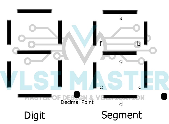
Fig 2: 7-Segment Display
7-segment displays are made up of 7 LEDs that are organised in such a way that they may display numerals ranging from 0 to 9. LEDs and 7-segment displays are both attached to the microcontroller, i.e., in series with a current limiting resistor.
The main difference is that they have 8 pins instead of 2 since each of the 7 LEDs has its own pin as well as a common cathode or anode pin. 7-segment screens are classified into two types:
7 Segment Display Common Anode
All LEDs of this kind share a single anode terminal, whereas each cathode terminal connects to a distinct section. To light a segment, the matching cathode terminal is grounded and the common anode terminal is supplied with +5V source power.
To connect a common anode type to a microcontroller, connect the cathodes of each segment via the microcontroller’s corresponding port pins.
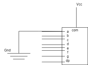
Fig 3: 7-Segment Display Common Anode
7 Segment Display Common Cathode:
All LEDs of this kind share a single cathode terminal, whereas each anode terminal connects to a distinct section. To light a segment, the appropriate anode terminal will be supplied with a +5V source voltage, while the common cathode terminal will be grounded. To link a common anode type to a microcontroller, the anodes of each segment are connected via the microcontroller’s corresponding port pins.
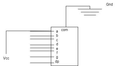
Fig 4: 7 Segment Display Common Cathode
Below is the Verilog of the 7-segment LEDs with FPGA
module Binary_To_7Segment
  (
   input       i_Clk,
   input [3:0] i_Binary_Num,
   output      o_Segment_A,
   output      o_Segment_B,
   output      o_Segment_C,
   output      o_Segment_D,
   output      o_Segment_E,
   output      o_Segment_F,
   output      o_Segment_G
   );

  reg [6:0]    r_Hex_Encoding = 7'h00;

  					// Case statement of each binary code
  always @(posedge i_Clk)
    begin
      case (i_Binary_Num)
        4'b0000 : r_Hex_Encoding <= 7'h7E;
        4'b0001 : r_Hex_Encoding <= 7'h30;
        4'b0010 : r_Hex_Encoding <= 7'h6D;
        4'b0011 : r_Hex_Encoding <= 7'h79;
        4'b0100 : r_Hex_Encoding <= 7'h33;
        4'b0101 : r_Hex_Encoding <= 7'h5B;
        4'b0110 : r_Hex_Encoding <= 7'h5F;
        4'b0111 : r_Hex_Encoding <= 7'h70;
        4'b1000 : r_Hex_Encoding <= 7'h7F;
        4'b1001 : r_Hex_Encoding <= 7'h7B;
        4'b1010 : r_Hex_Encoding <= 7'h77;
        4'b1011 : r_Hex_Encoding <= 7'h1F;
        4'b1100 : r_Hex_Encoding <= 7'h4E;
        4'b1101 : r_Hex_Encoding <= 7'h3D;
        4'b1110 : r_Hex_Encoding <= 7'h4F;
        4'b1111 : r_Hex_Encoding <= 7'h47;
      endcase
    end 							// always @ (posedge i_Clk)

  							// unused r_Hex_Encoding[7]
  assign o_Segment_A = r_Hex_Encoding[6];
  assign o_Segment_B = r_Hex_Encoding[5];
  assign o_Segment_C = r_Hex_Encoding[4];
  assign o_Segment_D = r_Hex_Encoding[3];
  assign o_Segment_E = r_Hex_Encoding[2];
  assign o_Segment_F = r_Hex_Encoding[1];
  assign o_Segment_G = r_Hex_Encoding[0];

endmodule 						// Binary_To_7Segment
In this blog, we learned about the interfacing of basic LEDs and 7-segment LEDs with FPGA, as well as some of its functionality.
So, let us summarise the entire blog in a few questions so that the facts are clearer.
- What exactly do you mean by FPGA?
- Explains how to construct and simulate flickering LEDs using HDL.
- What are 7-segment LEDs and how do they work?
- How to use FPGA to interface with 7-segment LEDs.