In my previous blog we already studied this, but let’s start with more energy and more explanation.
Verilog has several constructs for modelling switch-level circuits. These components are used to characterise digital circuits at the MOS-transistor level.
As Verilog supports transistor level modelling, designers use it these days since the complexity of circuits has forced them to go to higher levels of abstraction rather than switch level modelling.
At this level, a hardware component is specified at the transistor level, but transistors only display digital behaviour and have digital input and output signal values.
Transistors act as on-off switches at the switch level- Verilog employs a four-value logic value system, therefore Verilog switch input and output signals can take any of the four logic values (0, 1, Z, and X).
MOS switches
The terms “nmos” and “pmos” can be used to denote two types of MOS switches. The keywords nmos and pmos are used to model NMOS transistors and PMOS transistors, respectively. The figure depicts the symbols for nmos and pmos switches.
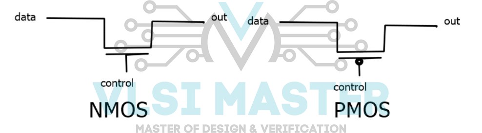
Fig 1: NMOS and PMOS
As demonstrated below, nmos and pmos switches are created in Verilog.
nmos n1(out, data, control); // instantiate a nmos switch
pmos p1(out, data, control); // instantiate a pmos switch
Because switches, like logic gates, are Verilog primitives, the instance name is optional. As a result, it is permissible to instantiate a switch without providing an instance name.
nmos (out, data , control); // instantiate nmos switch ; no instance name
pmos (out, data, control); // instantiate pmos switch; no instance name
The output signal’s value is determined by the values of the data and control signals. The following table displays the logic tables for out.
Some data and control signal combinations lead the gates to produce a 1 or a 0 or a z value with no preference for either.
The character L represents 0 or Z, while the symbol H represents 1 or z.
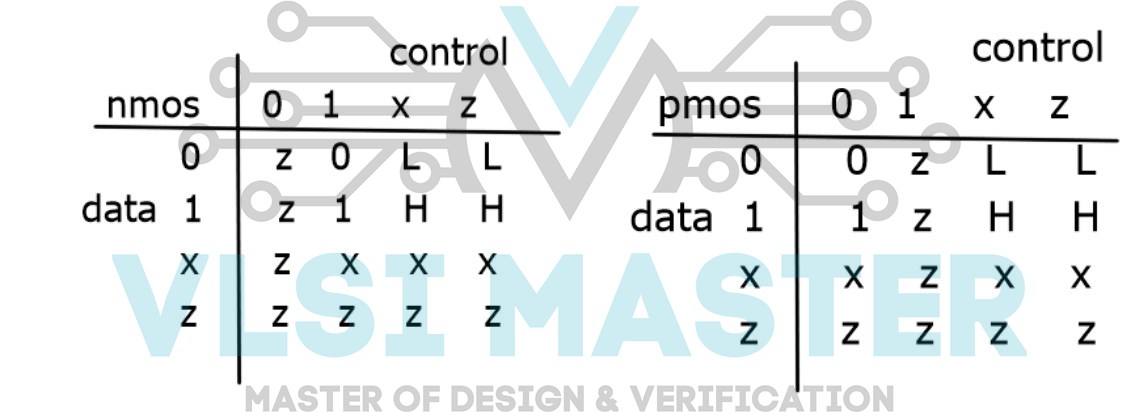
Fig 2: Logic Table of NMOS and PMOS
As a result, when the nmos switch’s control signal is 1, it conducts.
If the control signal is zero, the output has a high impedance value. Similarly, if the control signal is 0, a pmos switch conducts.
CMOS
The term “cmos” is used to identify CMOS switches. A CMOS device can be represented by an nmos and a pmos device. The figure depicts the symbol for a cmos switch.
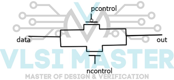
Fig 3: CMOS
As demonstrated below, a CMOS switch is created.
cmos cl(out, data, ncontrol, pcontrol);//instantiate cmos gate
or
cmos (out, data, ncontrol, pcontrol); //no instance name given
Normally, ncontrol and pcontrol are complementary.
The switch operates when the ncontrol signal is 1 and the pcontrol signal is 0. If ncontrol is 0 and pcontrol is 1, the switch’s output has a high impedance value.
The cmos gate is essentially a hybrid of two gates: a nmos and a pmos. As a result, the above cmos instantiation is identical to the following.
nmos (out, data, ncontrol); //instantiate a nmos switch
pmos (out, data, pcontrol); //instantiate a pmos switch
Because a cmos switch is generated from nmos and pmos switches, the output value may be calculated using the table, given data, ncontrol, and pcontrol signal values.
Bidirectional Switches
Gates such as NMOS, PMOS, and CMOS conduct from drain to source. It’s critical to have gadgets that can operate in both ways.
In such instances, the driving signal might come from either side of the device. For this reason, bidirectional switches are offered. Bidirectional switches are defined by three keywords: tran, tranif 0, and tranifl.
The symbols for these switches are depicted in the image below.
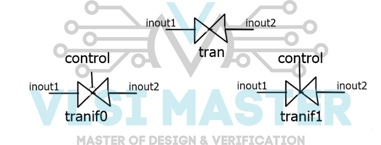
Fig 4: Bidirectional Switches
The tran switch acts as a buffer between the two signals inoutl and inout2. Either inoutl or inout2 can be the driver signal.
The tranif0 switch connects the two signals inoutl and inout2 only if the control signal is logical 0. If the control signal is a logical 1, the nondriver signal gets a high impedance value z.
The driver signal retains value from its driver. The tranifl switch conducts if the control signal is a logical 1.
These switches are instantiated as shown in below
tran tl(inoutl, inout2); //instance name tl is optional
tranifO (inoutl, inout2, control); //instance name is not specified
Resistive Switches
As previously stated, resistive devices include MOS, CMOS, and bidirectional switches. Because resistive switches have a higher source-to-drain impedance than conventional switches, the signal power that passes through them is reduced.
Resistive switches are denoted by keywords that are prefixed with a in comparison to the comparable keywords for ordinary switches.
The syntax of resistive switches is the same as that of ordinary switches.
rnmos		rpmos				// resistive nmos and pmos switches
rcmos						//resistive cmos switch
rtran		rtranif0		rtranif1		//resistive bidirectional switches.
Regular switches and resistive switches differ primarily in two ways: their source-to-drain impedances and how they pass signal intensities.
The source-to-drain impedance of resistive devices is quite high. The source-to-drain impedance of standard switches is low.
When signals flow via resistive switches, the signal strength is reduced. The modifications are depicted below.
Regular switches maintain signal intensity levels from input to output. The exception is that if the input is of supply strength, the output is of strong strength.
The strength reduction caused by resistive switches is seen in below table.
| Input Strength | Output Strength |
| Supply | Pull |
| Strong | Pull |
| Pull | Weak |
| Weak | Medium |
| Large | Medium |
| Medium | Small |
| Small | Small |
| High | High |
Example:
CMOS NOR gate
Even though Verilog has a nor gate primitive, let us create our own using CMOS switches. Figure 6 depicts the nor gate’s gate and switch-level circuit diagram.
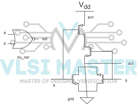
Fig 6 : Gate and Switch Diagram of NOR gate
The following is a description of verilog.
//Define our own nor gate, my_nor
module my_nor(out, a, b);

output out;
input a, b;

//internal wires
wire c;

//set up power and ground lines
supply1 pwr; //pwr is connected to Vdd (power supply)
supply0 gnd ; //gnd is connected to Vss(ground)

//instantiate pmos switches
pmos (c, pwr, b);
pmos (out, c, a);

//instantiate nmos switches
nmos (out, gnd, a);
nmos (out, gnd, b);

endmodule
Using the simulator shown below, we can demonstrate and test our nor gate.
// stimulus to test the gate
module stimulus;
reg A, B;
wire OUT;

//instantiate the my_nor module
my_nor n1(OUT, A, B);

//Apply stimulus
initial
begin
    //test all possible combination
    A =1’b0 B = 1’b0;
    #5 A =1’b0 B = 1’b1;
    #5 A =1’b1 B = 1’b0;
    #5 A =1’b1 B = 1’b1;
end

//check module
initial
        $monitor($time, “ OUT = %b, A = %b, B = %b, OUT, A, B);
endmodule
The output of the above example is shown below in the figure, and we hence construct no gate
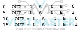
Fig 7 NOR gate output
Verilog strength Example
When the ‘OR’ and ‘AND’ operations below drive the same output, the final strength of the output is the strongest driver.
or (supply1, pull0) o1(out, i1, i2)
and (strong1, supply0) a1(out, i1, i2)
| Input driven | Output strength | Description |
| i0 = 0, i1 = 0 | out = 0 (pull0) | pull0 strength (= 5) > weak0 strength (=3) |
| i0 = 0, i1 = 1 | out = x | The out net is driven as 0 (supply0) and 1 (supply1) simultaneously. |
| i0 = 1, i1 = 0 | out = x | The out net is driven as 0 (supply0) and 1 (supply1) simultaneously. |
| i0 = 1, i1 = 1 | out = 1 (supply1) | supply1 strength (= 7) > strong1 strength (=6) |
The following is a description of verilog.
module strength(
  input i1, i2,
  output out);

  //assign (supply1, pull0) out = (i1 | i2);
  //assign (strong1, supply0) out = i1 & i2;

  or (supply1, pull0) o1(out, i1, i2);
  and (strong1, supply0) a1(out, i1, i2);

endmodule
The output of the above example is shown below in the figure8.
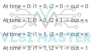
Fig 8 Verilog strength Example
So, from this blog, we now have a clear understanding of switch modelling elements and can easily explain them to others.
So let’s summarize the whole blog with a few questions so that all of the concepts will be crystal clear.
- What exactly are these switch modelling elements?
- What do you mean by MOS switches, and what are their different types?
- What exactly is CMOS, and how does it vary from CMOS?
- What do you mean by bidirectional switches, and what are the different types?
- What exactly do you mean by “resistive switches”?