So far we have read blogs about some of the basics about Verilog. Now we will see some interesting facts about Verilog in this blog, which are very basic in the design process of Verilog HDL. Let’s start with the module, which is its most important and basic fact regarding Verilog HDL design flow
Module
The idea of a module is provided by Verilog. In Verilog, a module is the fundamental building unit. A module can be either an element or a grouping of lower-level design pieces. Elements are frequently categorised into modules to offer common functionality that is required across the design.
A module exposes the underlying implementation while providing the essential functionality to the higher-level block via its port interface (inputs and outputs). This permits the developer to change the internals of the module without impacting the further design.
Types of module
Verilog is a behavioural as well as a structural language. Depending on the demands of the design, the internals of each module can be specified at four levels of abstraction.
Regardless of the level of abstraction used to describe the module, it operates in the same way with the external environment. The module’s internals are concealed from the outside world. As a result, the level of abstraction used to define a module can be changed without having any effect on the environment.
Let’s discuss types in a brief way as it introduces you to the design flow of Verilog HDL and it will be explained clearly in other blogs.
- Behavioral or Algorithmic Level: The Verilog HDL provides the highest level of abstraction. Without regard to hardware implementation specifics, a module can be built in terms of the intended design algorithm. This level of design is fairly close to C programming.
- Dataflow Level: The module is designed at this level by specifying the data flow. The designer understands how data travels between hardware registers and how data is handled in the design.
- Gate Level: The module is implemented in terms of logic gates and their connections. This level of design is similar to expressing a design in terms of a gate-level logic diagram.
- Switch Level: At the lowest degree of abstraction, Verilog provides the A module can be built in terms of switches, storage nodes, and their interconnections. Designing at this level necessitates understanding of switch level implementation details.
Verilog allows the designer to combine all four levels of abstraction into a single design. The term register transfer level (RTL) is commonly used in the digital design field to refer to a Verilog description that includes a combination of behavioural and dataflow components and is compatible with logic synthesis tools.
Instances
A module serves as a template from which actual objects can be created. When a module is called, Verilog generates a one-of-a-kind object from the template. Each object is distinguished by its own name, variables, arguments, and I/O interface.
The act of constructing objects from a module template is known as instantiation, and the objects themselves are known as instances.
Nesting modules is not permitted in Verilog. A module definition cannot include another module definition within the module and endmodule commands. Instead, a module definition can include copies of other modules by instantiating them.
Simulation
When a design block is finished, it must be tested. The design block’s functioning may be tested by applying a stimulus and observing the outcomes. This type of block is known as a stimulus block. It’s best to keep the stimuli and design blocks distinct. Verilog may be used to write the stimulus block.
It is not necessary to use a different language to describe stimulation. The stimulus block is also known as a test bench. To completely evaluate the design block, many test benches might be employed.
There are only two possible styles of stimulus application.

Fig 1: Stimulus Block Instantiates Design Block
The stimulus block in the first style instantiates the design block and directly drives the signals in the design block. The stimulus block is elevated to the top-level block in Figure 1. It manipulates the signals CLK and reset, as well as checks and displays the output signal q.
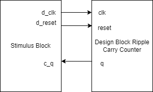
Fig 2: Stimulus and Design Blocks Instantiated in a Dummy Top- Level Module
The second approach is to instantiate both the stimulus and design blocks in a top-level example module. The stimulus block only communicates with the design block via the interface.
Figure 2 depicts this method of providing stimuli. The stimulus module drives the signals d clk and d reset, which are coupled to the design block’s signals clk and reset.
It also examines and displays signal c_q, which is linked to signal q in the design block. The top-level block’s role is merely to instantiate the design and stimulus blocks.
Logic Synthesis
HDLS has risen to the forefront of digital design technology thanks to advances in logic synthesis. Logic synthesis technologies have considerably reduced design cycle times. Designers may work at a high degree of abstraction, reducing design time.
Simply said, logic synthesis is the process of transforming a high-level design description into an optimised gate-level representation, given a standard cell library and certain design limitations.
Simple cells, such as and, or, and nor logic gates, can be found in a conventional cell library, as can macro cells, such as adders, muxes, and special flip-flops. A technology library is another name for a standard cell library. It will be covered in greater depth later.
Even in the days of schematic gate-level design, logic synthesis existed, but it was always done in the designer’s head. The designer would begin by comprehending the architectural description.
Then they think about design restrictions like time, area, testability, and power. The designer would divide the design into high-level pieces, sketch them on paper or a computer terminal, and describe the circuit’s operation.
This was the high-level summary. Finally, each block would be built on a hand-drawn schematic utilising the standard cell library’s cells.
The final phase was the most difficult in the design cycle, requiring numerous time-consuming design iterations before obtaining an optimal gate-level representation that fulfilled all design criteria.
As seen in Figure 3, the designer’s thoughts were employed as a logic synthesis tool.

Fig 3 Logic synthesis mapping
What we learn from today’s blog, we see them in the form of some questions so that our facts will be remembered even better.
- What are the basics of Verilog HDL design flow?
- What do you mean by module in Verilog?
- What are the types of modules in Verilog?
- What are Instances?
- What is simulation and how many types of simulation in Verilog?